
Global Main Site
Foundry Access for Global Chip Teams
From design support and IP through MPW, NTO, packaging, test and delivery, TOMPW Service supports the full semiconductor path for startups, labs and production programs worldwide.
Why Teams Choose TOMPW
One coordination point
Across design support, foundry access, packaging, test and delivery — your team manages one relationship instead of five.
Full delivery-path coverage
From MPW and NTO through full mask, plus packaging, test, PCB and turnkey execution.
Asia-based, globally reachable
Execution anchored in Asia with global communication and delivery coordination.
Semiconductor service operation
Core service lines
Standard process coverage
Engagement models
Engagement Models
Start with MPW, scale to NTO or full mask
Prototype silicon through MPW, validate with engineering runs, then ramp to production — with package and test support at every stage.
MPW
Shared-mask shuttle access for prototype silicon, cost-sensitive validation runs and early customer sampling.
NTO / Engineering Run
A transition path for teams that need more control than MPW but are not yet ready for a full production commitment.
Full Mask
Dedicated production engagement for programs that already have a clearer forecast, package path and ramp objective.
Service Catalog
12 service lines across the silicon delivery chain
From architecture to shipped product — design, IP, foundry access, packaging, test and turnkey delivery.
Tape-out & Foundry Access
MPW, NTO and full-mask shuttles across 29 partner fabs.
LOWER NRE · FASTER FIRST SILICON
MPW / Fab Shuttle
Compare public shuttle windows across foundries, control first-silicon cost and move from tape-out planning to wafer delivery with one execution path.
PRODUCTION RAMP · DEDICATED MASK SET
Full Mask / Production Foundry
Move validated designs into dedicated mask production with yield, volume and supply planning support.
Design, IP & Engineering
ASIC/SoC architecture, verification, physical design and licensable IP cores.
ARCHITECTURE TO RTL
ASIC / SoC Design
Support architecture, RTL and integration planning for teams moving from specification to implementation.
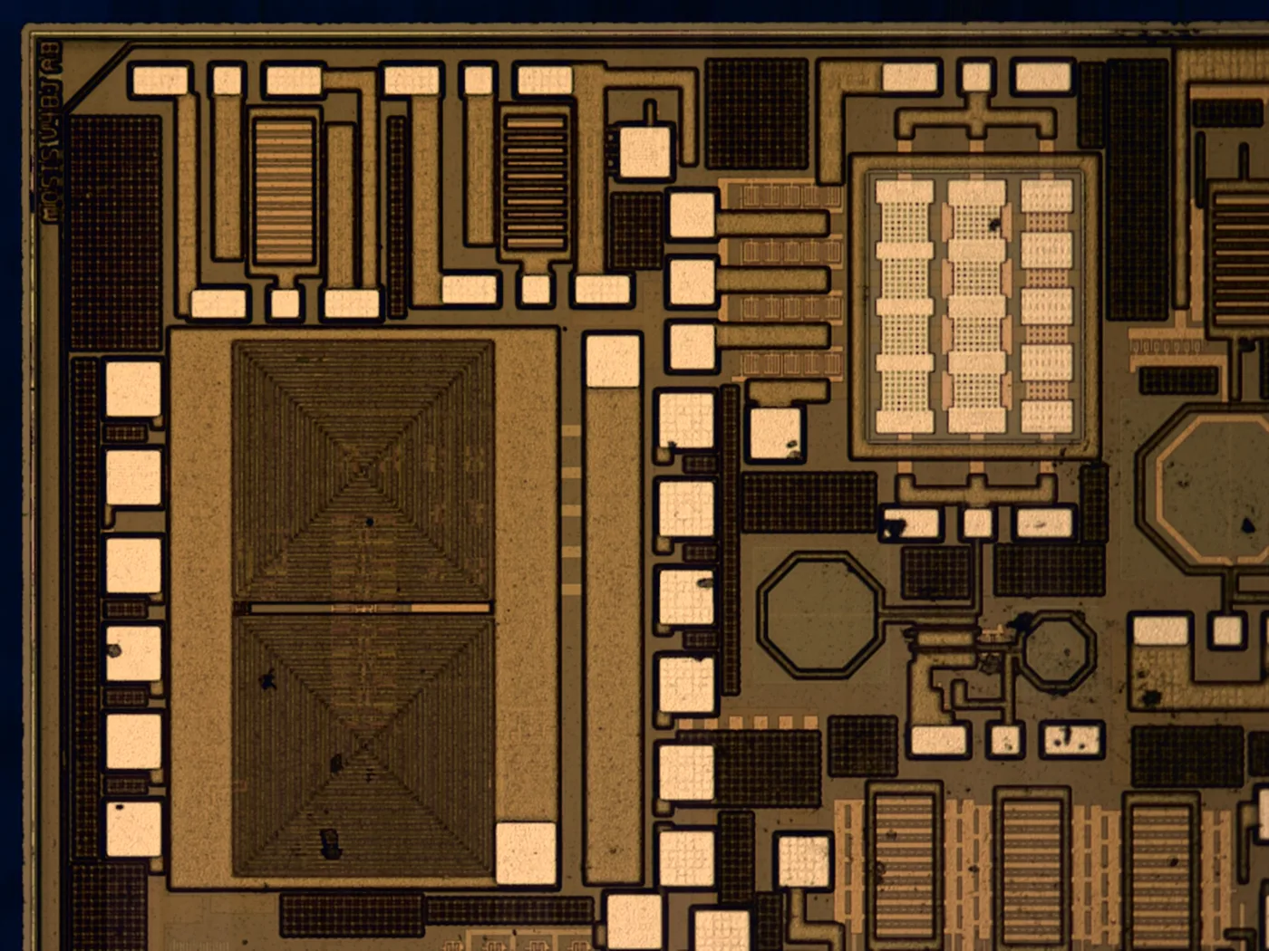
FIRST-SILICON CONFIDENCE
Design Verification
Strengthen first-silicon confidence with structured verification, validation planning and downstream debug preparation.
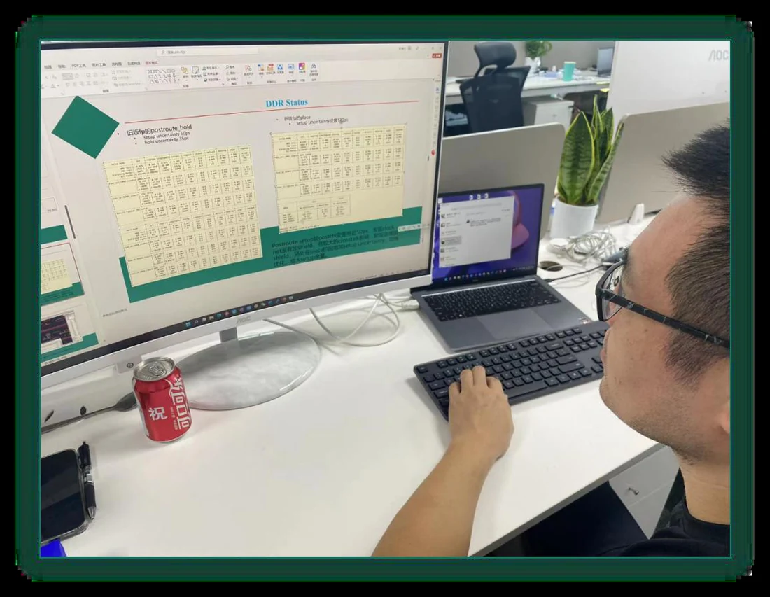
BACKEND TO SIGN-OFF
Physical Design & Layout
Bridge netlist to manufacturable layout with backend planning that stays aligned with foundry rules and sign-off needs.
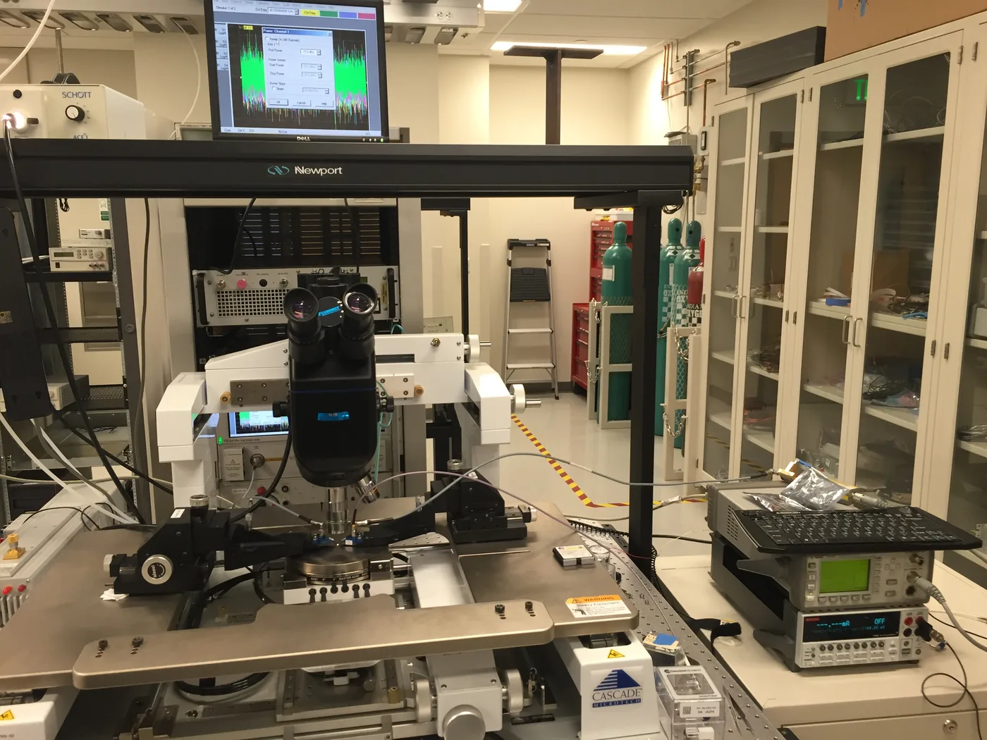
IP FIT BEFORE INTEGRATION PAIN
IP Cores & Licensing
Reduce schedule risk by aligning interface, memory and subsystem IP choices with the actual process and integration path.
Packaging, Test & Delivery
Packaging, test, PCB, firmware, supply chain and turnkey productization.
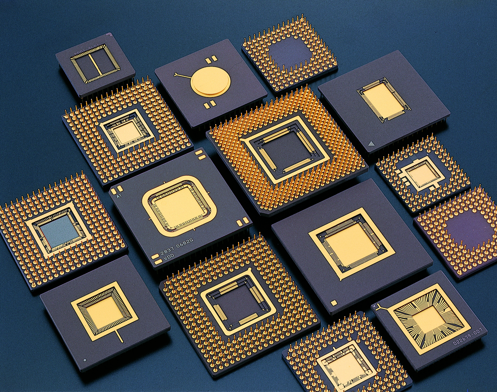
ASSEMBLY PATH TO SHIPPABLE PRODUCT
Semiconductor Packaging
Plan package type, prototype assembly, inspection and qualification early so silicon delivery does not stall after wafer completion.
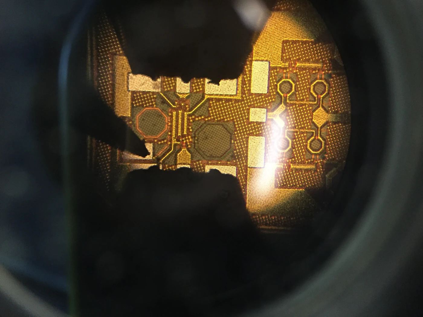
CP · FT · RELIABILITY
Test & Product Engineering
Connect CP, FT and reliability planning so packaged silicon is measurable, debuggable and ready for customer evaluation.
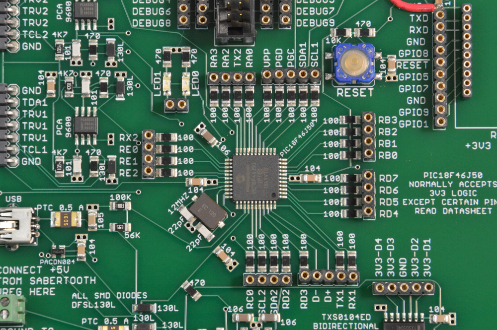
BOARD-LEVEL PRODUCTIZATION
PCB Design & Manufacturing
Support evaluation boards, demo boards and production-minded PCB work that connects packaged silicon to a usable system.
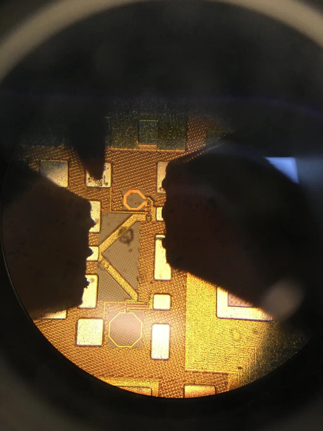
BRING-UP TO DEMO
Embedded Software & Firmware
Connect chip bring-up with firmware, board support and system validation so custom silicon can be demonstrated quickly.
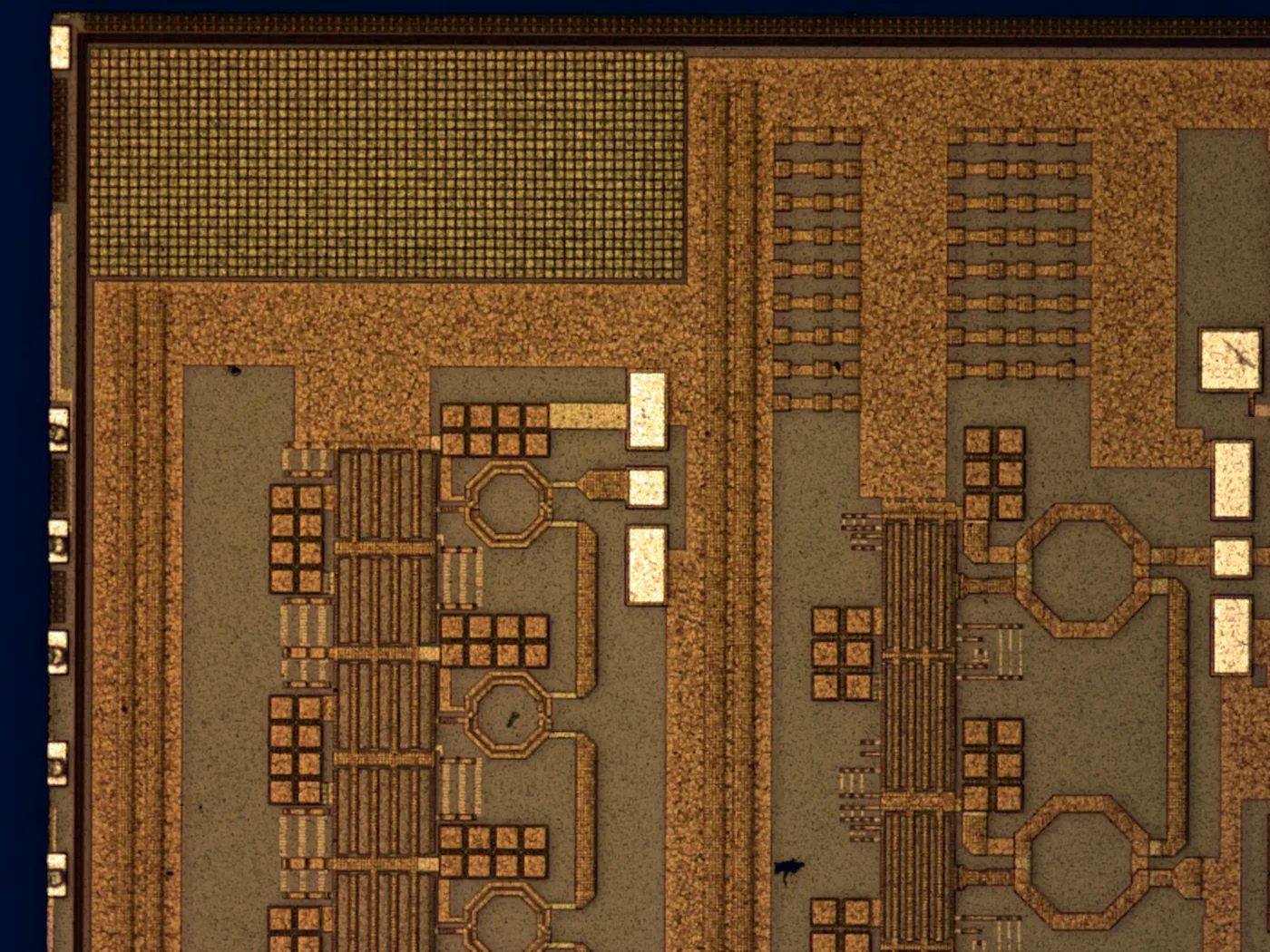
ONE COORDINATED CHAIN
Supply Chain & Logistics
Simplify handoffs across fabs, packaging houses, test providers and international delivery partners.
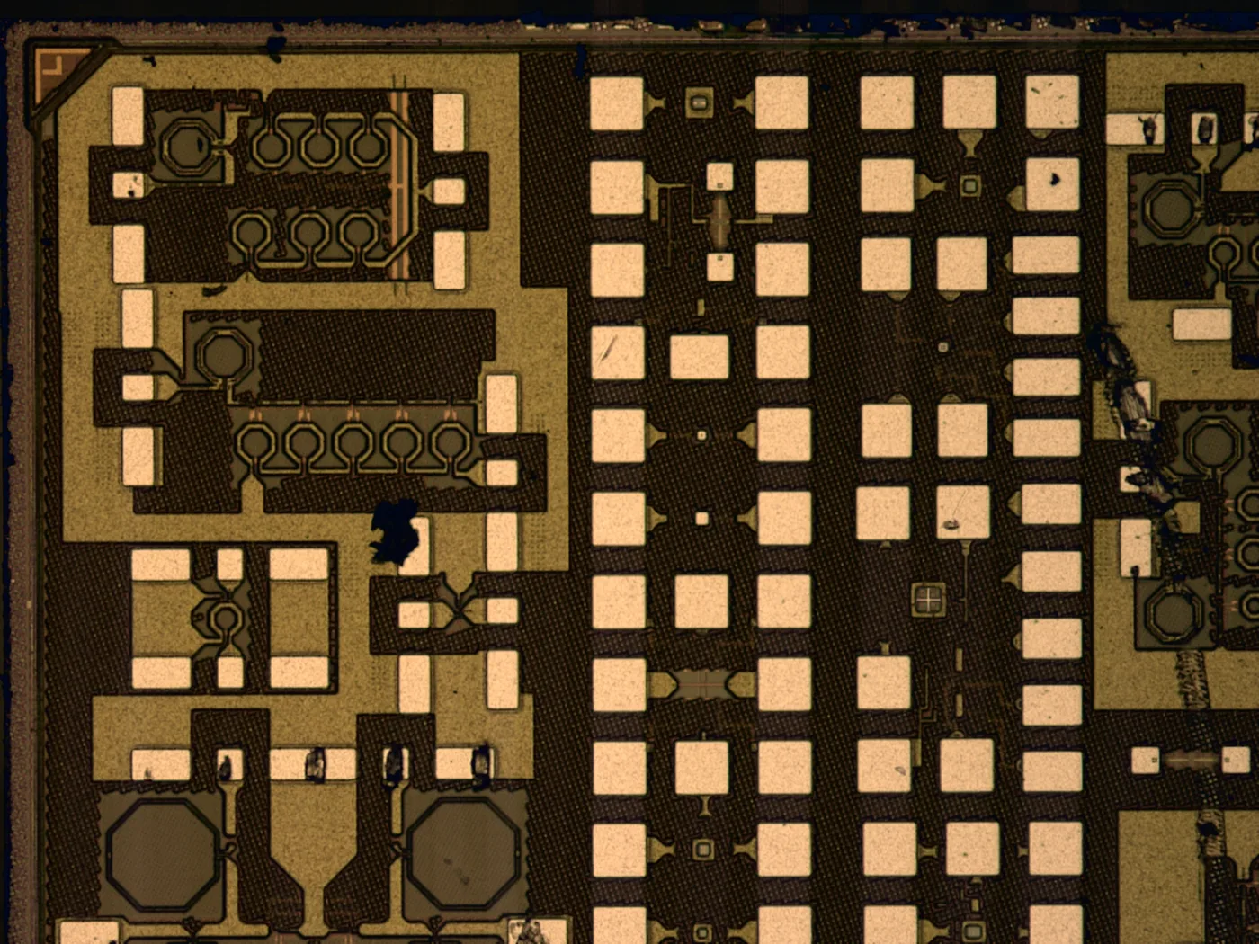
ONE PARTNER · FULL DELIVERY PATH
Turnkey ASIC Solutions
Unify design support, tape-out, packaging, test, board work and delivery under one execution-facing partner.
Process Platform Coverage
Technology references span the mainstream and specialty landscape
Foundry and Process Coverage
Real foundry and process coverage, shown in detail
Documented process coverage
- Standard process coverage highlighted in current source material spans 12nm to 3um.
- Below-7nm programs are evaluated case by case based on ecosystem fit, schedule and commercial model.
- Common platform references include CMOS, BCD, SOI, SiGe, GaAs, GaN, silicon photonics and MEMS.
Browse foundries by process and node

























CALCULATORS
Plan your tape-out with free calculators
Die Per Wafer Calculator
Estimate gross and net dies per wafer from wafer size, die dimensions, scribe lanes, edge exclusion and yield models.
Open toolMPW Cost Sharing Calculator
Split a shared MPW wafer cost across multiple designs by occupied wafer area — per-participant share and cost.
Open toolWafer & Unit Cost Calculator
Turn a wafer run into a per-chip cost: dies per wafer, yield, packaging and test, plus a target margin.
Open toolNode / Wafer DPW Comparison
Compare dies per wafer and cost per die across 100/150/200/300 mm wafers for a fixed die.
Open toolTape-out Budget Estimator
Full program model: DPW, yield, packaging, HBM, test, NRE and volume → unit cost, price and gross margin.
Open toolPackage Selection Advisor
Match QFN, BGA, WLCSP, Flip-Chip, SiP or legacy leaded packages to your IO, power, RF, cost and form-factor constraints.
Open toolTest Cost & Yield Calculator
Estimate ATE test cost per device and per good unit from tester rate, test time, handler cost, volume and test yield.
Open toolRecent Updates
Latest insights and foundry coverage notes
MPW window updates, process node coverage notes and delivery chain guidance for teams planning their next tape-out.
- July 9, 2026MPW4 min read
Why packaging lead times should be reviewed before MPW slot confirmation
Packaging is often treated as a post-tape-out task, but for many MPW programs the real schedule risk starts much earlier.
Read update - June 15, 2026TSMC4 min read
TSMC N3X Node Opens New MPW Window for AI Edge Prototyping
TSMC's N3X node is now accessible through MPW shuttle programs, giving AI edge chip teams a lower-risk path to advanced-node silicon validation.
Read update - May 20, 2026SMIC5 min read
SMIC 28nm MPW: A Cost-Effective Path for IoT and Industrial ASIC Programs
SMIC's 28nm platforms remain one of the most cost-effective entry points for IoT and industrial ASIC programs that need mature yield and global supply chain access.
Read update
Latest visible update
July 9, 2026
Dated updates tracked
3
Update topics covered
13
Execution Path
From slot to shipped silicon
The TOMPW workflow follows a practical delivery chain rather than a single-handoff model. Each stage below is backed by real project materials and documented outcomes.
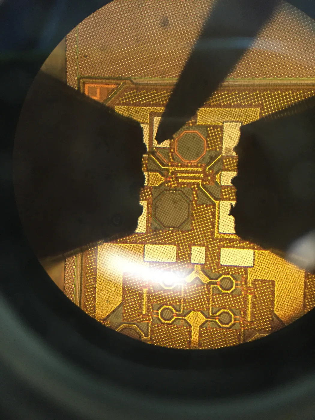
Design & Tape-out Readiness
Process window confirmation, DRC/LVS sign-off readiness and GDS handoff coordination with the target foundry.
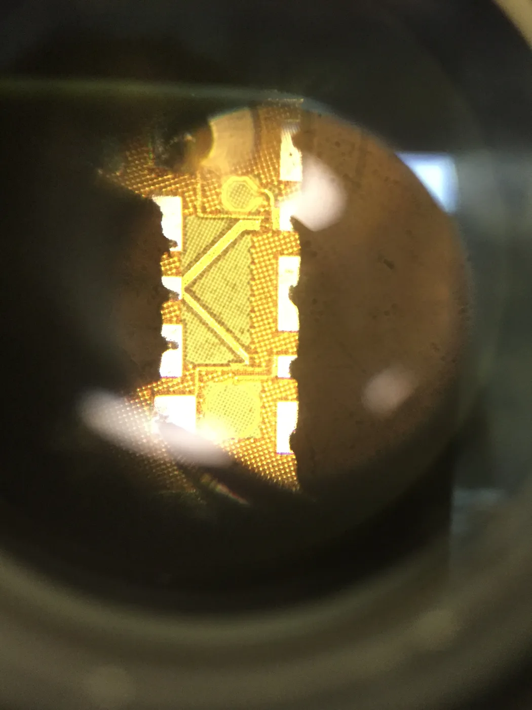
MPW Shuttle / Wafer Run
Slot enrollment, shuttle window tracking, mask ordering and wafer-in notification across multiple foundries.
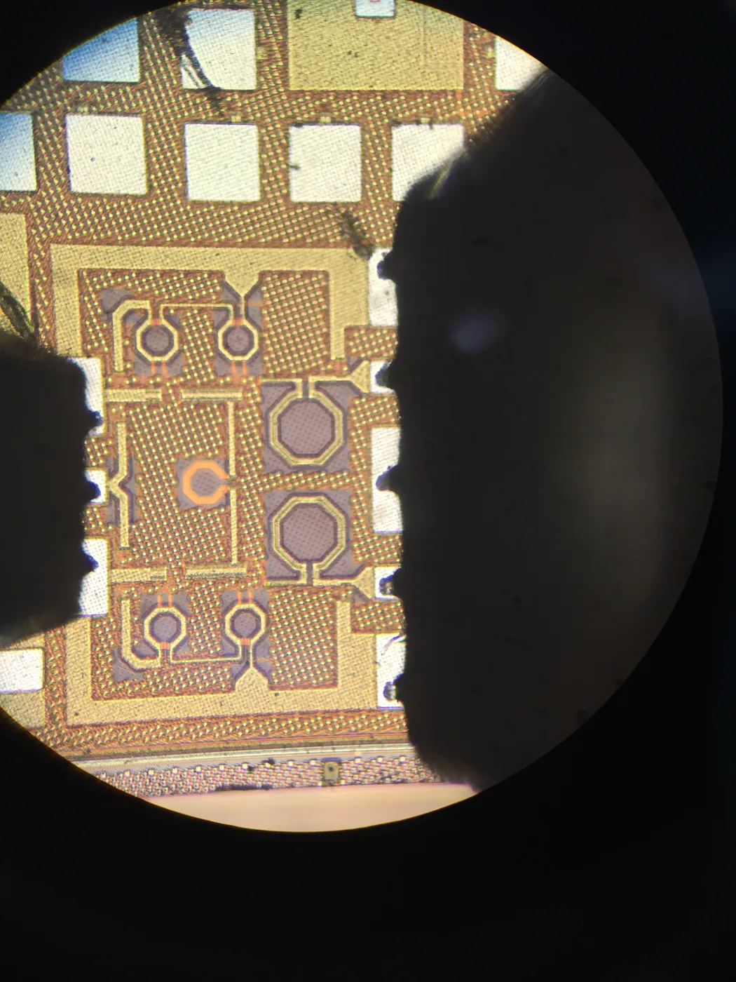
Probe & Test
Wafer receipt logging, probe program setup, parametric test data collection and first-silicon electrical validation.
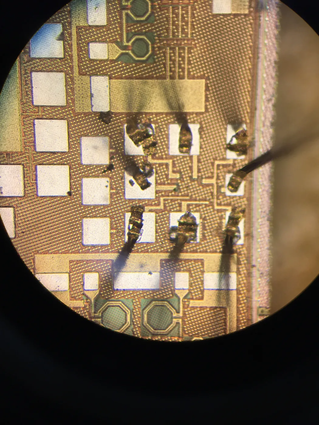
Package & Assembly
Package substrate selection, wire-bond or flip-chip path coordination, assembly house scheduling and incoming QA.
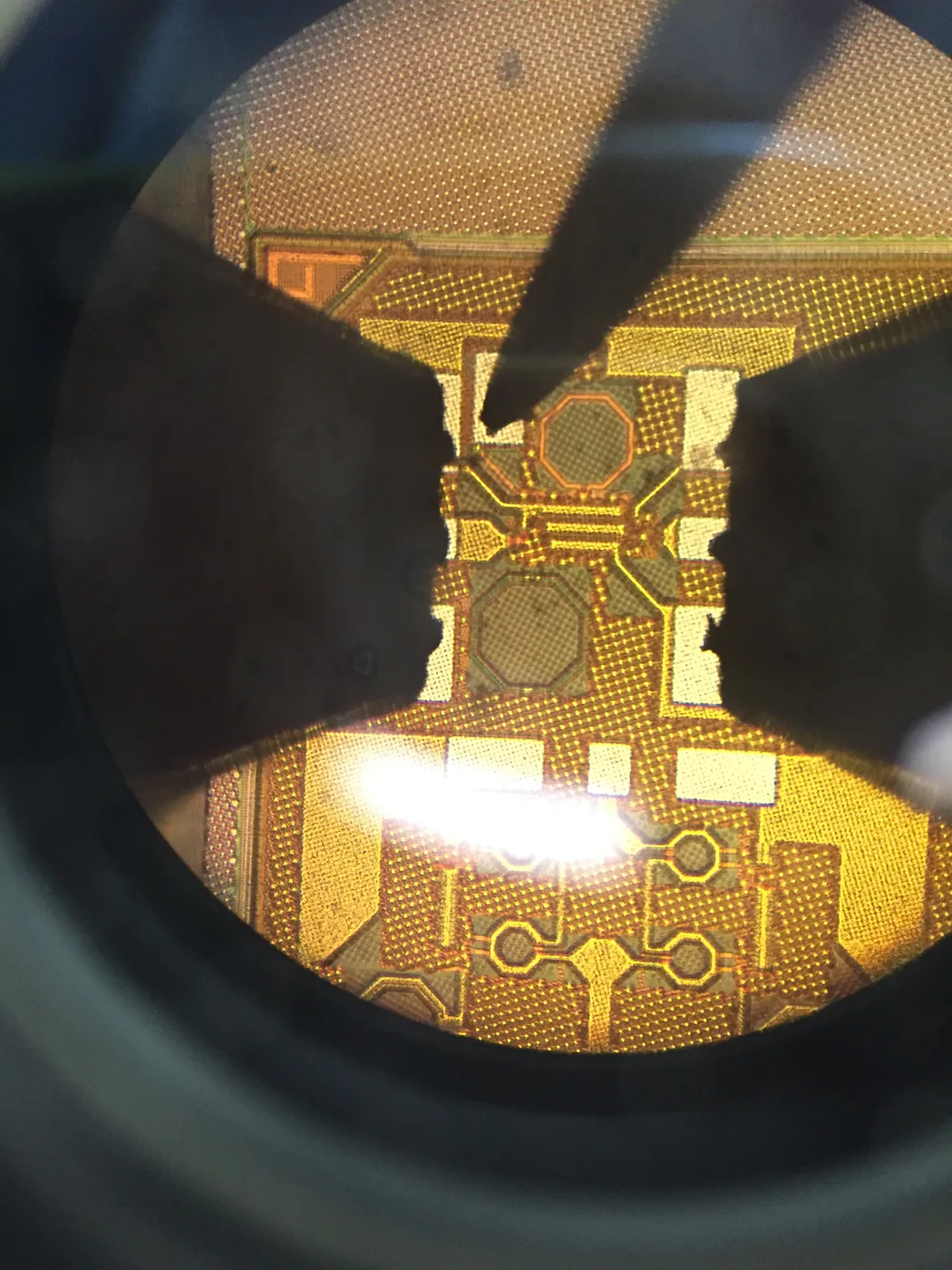
PCB & Bring-up
Board fabrication support, component sourcing, firmware loading assistance and post-silicon system integration help.
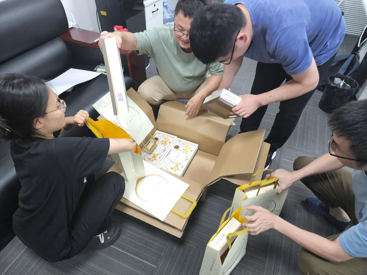
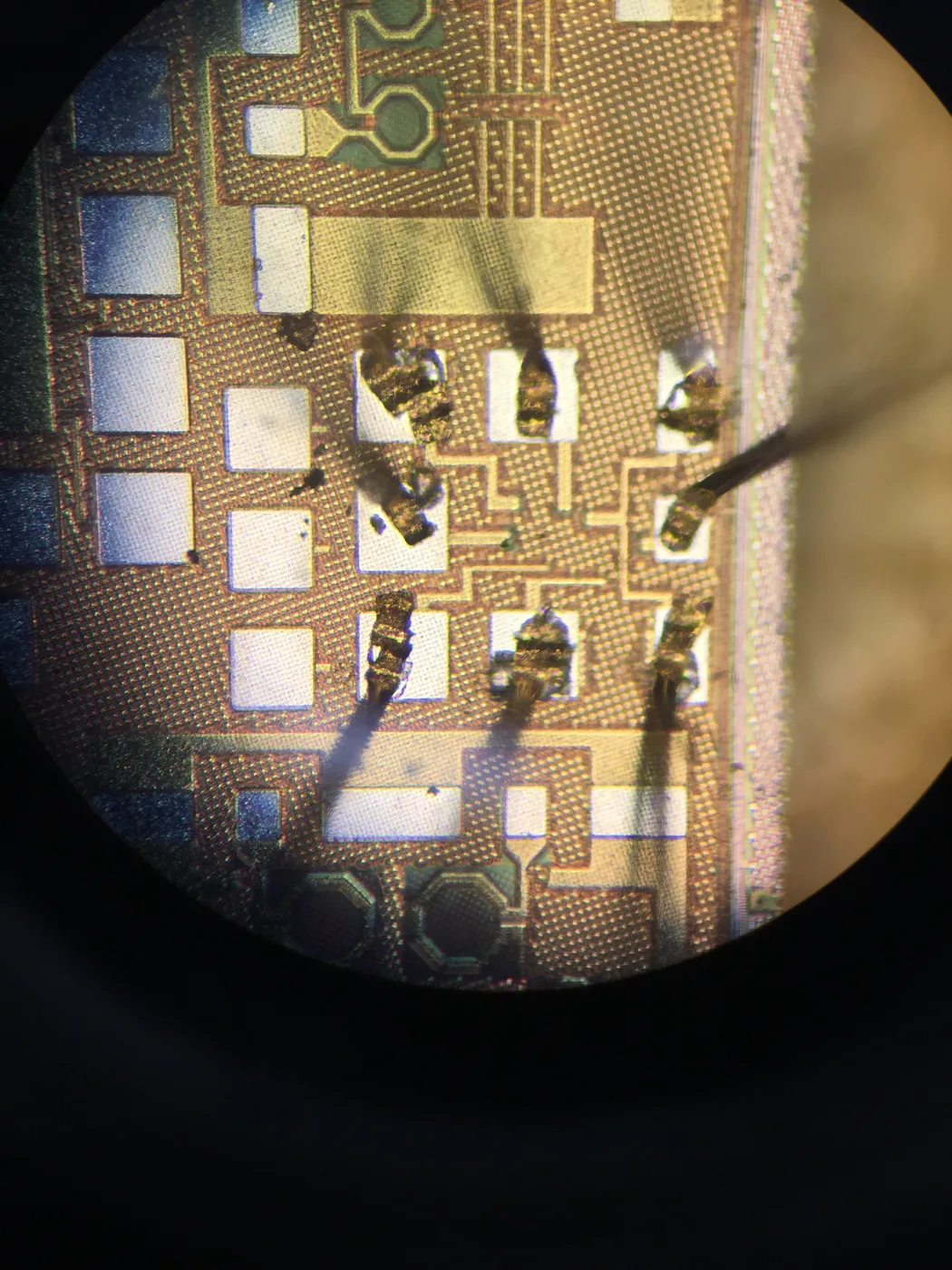
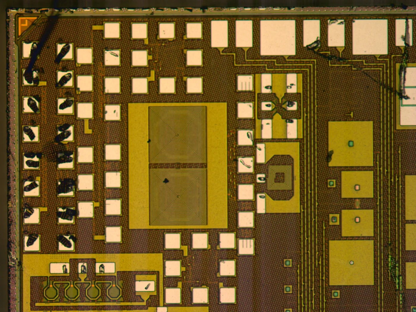
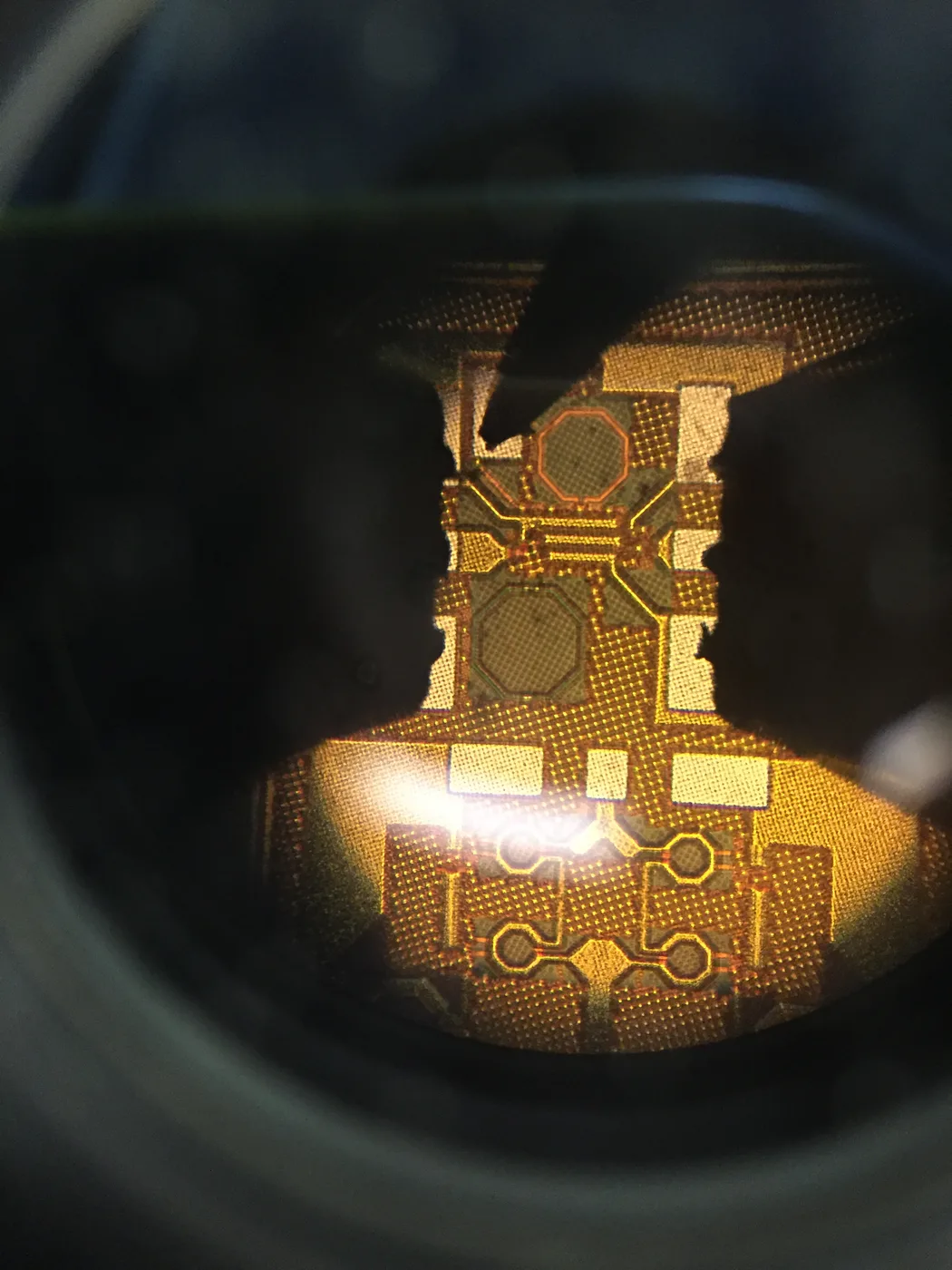
Photographs sourced from actual TOMPW-coordinated tape-out programs. Stages are illustrative — actual scope varies by project.
Questions Buyers Ask Before Tape-Out
Practical answers for planning foundry access and delivery
Answers to the questions chip teams typically ask before committing to MPW, package, test or a turnkey path.
TOMPW can enter at architecture and design, at netlist or GDS handoff, at tape-out and shuttle booking, or at packaging and test. What you need to provide depends on the entry point: usually the target node or an acceptable range, die size or a working estimate, package and test expectations, target quantity, and the dates that matter to you. Teams new to tape-out can start from a rough description and we will help shape the rest.
No. The broader value proposition includes MPW, NTO, full mask, packaging, test, PCB support, firmware support and turnkey execution coordination. TOMPW acts as an execution partner across the delivery chain, not only a wafer-order channel.
The current coverage spans 12nm to 3um, with some sub-7nm opportunities handled case by case. Node support is matched to each program through the foundry and MPW pages, so the range reflects real accessible platforms rather than a fixed catalog.
Start with the service pages to understand scope, then the foundry and MPW sections for process and scheduling context, then the guides for packaging, test and turnkey decisions. Each page is written to answer a concrete engineering or sourcing question, so you can move from question to scoped quote.
Next Step
Send node, package and schedule context first. We can scope the right path after that.
A strong first inquiry usually includes application, process range, project stage, target volume and whether package, test, PCB or firmware support are also needed.